Four Stages of PCB Design and Assembling
#PCBassembly #PrintedCircuitBoard #PCBBoard #PCBAssembly #smtassembly #pcbassemblyservices
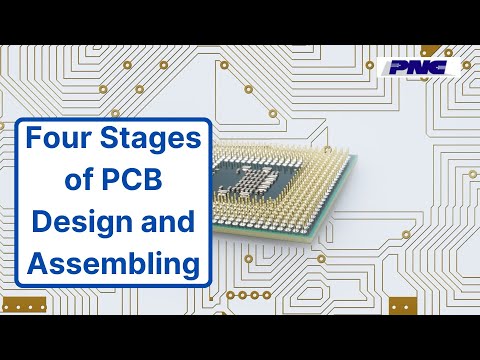
PCB is a printed circuit board that helps connect different electrical components. The board is a combination of laminated material, and the copper foil laid on a non-conductive substrate.
A PCB is the main part of any electronic device, so it has to be perfect. It should have functional components and microelectronics circuits to perform well. Development of PCB goes through different processes that you should know well. PCB manufacturing has 4 stages, including design, manufacturing, PCB assembly, and PCB testing.
First Stage- Design
PCB design involves different steps, such as schematic design, layout planning, the placement of the components, routing, and manufacturing files.
PCB schematic design: It is a blueprint of PC design that shows all PCB components with symbols. The schematic design is always according to the technical requirements of the user.
Layout planning: After the schematic design, you have to develop the layout of a PCB that includes physical components’ models, the shape of the PCB, and the structure of a PCB.
Placement of components: It involves planning the placement of various components. You decide on the PCB layers according to your requirements. The right placement of the components ensures a flawless board, decreasing the production cost.
First of all, the designer places the fixed components in the layout, including switches and connectors.
Then, the critical components are placed, such as memory chips, microprocessors, as well as power supplies.
Then the supporting components of the PCB are placed, like inductors, capacitors, and resistors.
In the end, the decoupling capacitors and terminating resistors are placed.
Routing: Once the components are placed, you have to connect all components through trace routing. There are four ways to do so, such as manual routing, auto-interactive routing, semi-automatic, and batch-auto routing. You can choose any method according to your Printed Circuit Board and budget.
Design: In this stage, you have to plan for the number of board layers, dimension of the board, and types of components. You can use a special app in this case, such as EDA or electronic design automation. The designer often adopts the SMT instead of a through-hole technology, depending on your requirements.Once the design is over, you can export the design files to CAD or Gerber format.
Preparation of manufacturing files: This is the last stage of design where the designer exports the Gerber files for manufacturing. The manufacturer needs these files to develop a printed circuit board.
Stage 2-Manufacturing of Circuit Board
Once the manufacturer receives all design drawings, he starts making PCB. It involves different stages as described below:
Design Imaging: The manufacturer uses a plotter to convert the PCB design files into filmslike they resemble the photo negatives of the schematic design. The printer uses black and clear inks for inner and outer layers. Copper traces and circuits are shown with black ink, whereas the non-conductive parts are shown with clearink.
Printing of Inner Layers on Copper: It is the initial stage of PCB manufacturing. The engineer uses a substrate material to make a laminated board. Like, epoxy resin or fiberglasses are common in this case. The design of the PCB is printed on the board, and then his pre-bondscopper on a board’s both sides. After that comes the etching of copper, and then the board is protected through a photo-sensitive film.
Ultraviolet Light: the manufacturer then exposes the resist-covered PCB to UV light to strengthen the photo-reactive material. Then the board is cleaned with an alkaline solution to get rid of unnecessary copper particles. The expert checks the board to remove any errors and then goes to the next stage. The main aim of UV blasting is to develop a PCB Board according to the schematic drawing.
Inner layer’s etching: copper’s inner layer needs chemical etching for removal. The process of photoresist prevents the essential copper from etching. The board size determines the amount of the solution and etching time which is less for small boards but more for large boards.
Read more:
https://bit.ly/3bUkSaE
Website:
https://pnconline.com/
Facebook:
https://www.facebook.com/PNCONLINE
Twitter:
https://twitter.com/PNCINC
Instagram:
https://www.instagram.com/pnc_pcb/
Tumblr:
https://www.tumblr.com/blog/view/pncinc
Myspace :
https://myspace.com/pncinc2020
Bresdel:
https://bresdel.com/pncinc
Pinterest :
https://www.pinterest.com.au/rrosh2014/_created/
Call us: (973) 284-1600
Email us: sales@pnconline.com
Location: PNC INC, 115 East Centre St.Nutley, NJ, 07110
Four Stages of PCB Design and Assembling
#PCBassembly
#PrintedCircuitBoard
#PCBBoard
#PCBAssembly
#smtassembly
#pcbassemblyservices
PCB is a printed circuit board that helps connect different electrical components. The board is a combination of laminated material, and the copper foil laid on a non-conductive substrate.
A PCB is the main part of any electronic device, so it has to be perfect. It should have functional components and microelectronics circuits to perform well. Development of PCB goes through different processes that you should know well. PCB manufacturing has 4 stages, including design, manufacturing, PCB assembly, and PCB testing.
First Stage- Design
PCB design involves different steps, such as schematic design, layout planning, the placement of the components, routing, and manufacturing files.
PCB schematic design: It is a blueprint of PC design that shows all PCB components with symbols. The schematic design is always according to the technical requirements of the user.
Layout planning: After the schematic design, you have to develop the layout of a PCB that includes physical components’ models, the shape of the PCB, and the structure of a PCB.
Placement of components: It involves planning the placement of various components. You decide on the PCB layers according to your requirements. The right placement of the components ensures a flawless board, decreasing the production cost.
First of all, the designer places the fixed components in the layout, including switches and connectors.
Then, the critical components are placed, such as memory chips, microprocessors, as well as power supplies.
Then the supporting components of the PCB are placed, like inductors, capacitors, and resistors.
In the end, the decoupling capacitors and terminating resistors are placed.
Routing: Once the components are placed, you have to connect all components through trace routing. There are four ways to do so, such as manual routing, auto-interactive routing, semi-automatic, and batch-auto routing. You can choose any method according to your Printed Circuit Board and budget.
Design: In this stage, you have to plan for the number of board layers, dimension of the board, and types of components. You can use a special app in this case, such as EDA or electronic design automation. The designer often adopts the SMT instead of a through-hole technology, depending on your requirements.Once the design is over, you can export the design files to CAD or Gerber format.
Preparation of manufacturing files: This is the last stage of design where the designer exports the Gerber files for manufacturing. The manufacturer needs these files to develop a printed circuit board.
Stage 2-Manufacturing of Circuit Board
Once the manufacturer receives all design drawings, he starts making PCB. It involves different stages as described below:
Design Imaging: The manufacturer uses a plotter to convert the PCB design files into filmslike they resemble the photo negatives of the schematic design. The printer uses black and clear inks for inner and outer layers. Copper traces and circuits are shown with black ink, whereas the non-conductive parts are shown with clearink.
Printing of Inner Layers on Copper: It is the initial stage of PCB manufacturing. The engineer uses a substrate material to make a laminated board. Like, epoxy resin or fiberglasses are common in this case. The design of the PCB is printed on the board, and then his pre-bondscopper on a board’s both sides. After that comes the etching of copper, and then the board is protected through a photo-sensitive film.
Ultraviolet Light: the manufacturer then exposes the resist-covered PCB to UV light to strengthen the photo-reactive material. Then the board is cleaned with an alkaline solution to get rid of unnecessary copper particles. The expert checks the board to remove any errors and then goes to the next stage. The main aim of UV blasting is to develop a PCB Board according to the schematic drawing.
Inner layer’s etching: copper’s inner layer needs chemical etching for removal. The process of photoresist prevents the essential copper from etching. The board size determines the amount of the solution and etching time which is less for small boards but more for large boards.
Read more: https://bit.ly/3bUkSaE
Website: https://pnconline.com/
Facebook: https://www.facebook.com/PNCONLINE
Twitter: https://twitter.com/PNCINC
Instagram: https://www.instagram.com/pnc_pcb/
Tumblr: https://www.tumblr.com/blog/view/pncinc
Myspace :https://myspace.com/pncinc2020
Bresdel: https://bresdel.com/pncinc
Pinterest :https://www.pinterest.com.au/rrosh2014/_created/
Call us: (973) 284-1600
Email us: sales@pnconline.com
Location: PNC INC, 115 East Centre St.Nutley, NJ, 07110