https://www.topscompcbassembly.com/en/contract-electronics-manufacturing-services-china-supplier/
PCBs And PCBA & Turnkey Electronics Contract Manufacturing Services & OEM ODM Supplier
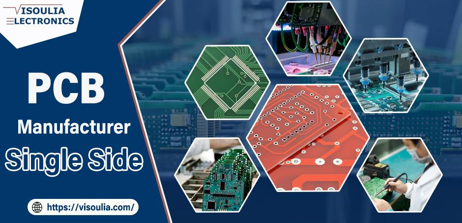
Topscom Technology, based on Shenzhen City, Guangdong (Canton) Province, China, is the best China PCB supplier you can count on. We specialize in providing complete engineering, supply chain, testing, and manufacturing services to global based customers. Our electronic contract manufacturing services include China PCB fabrication, PCB assembly, electro-mechancial assembly, mechanical tooling manufacturing, plastic injection molding, metal stamping, die-casting, final box build and system integration, function testing, burn in, and other custom China PCB fabrication.
https://cutt.ly/qwSD5hV0
PCB SMT assembly, China printed circuit board assembly, China PCB factory, China PCB fabrication, China PCB manufacturing, China PCB board, China PCB manufacturer, China PCB service, China PCB prototype, China PCB supplier, China PCB, PCB China, China PCB online, PCB board, China PCB assembly, PCBA China, China PCB design, PCB assembly, China PCB quote, PCBA, contract manufacturing China, China contract manufacturing, contract manufacturing, China electronic assembly, China electronic manufacturing, electronics manufacturing, electronic board manufacturers, China OEM manufacturing, OEM manufacturing
#electronic_board_manufacturers #PCB_SMT_assembly #China_PCB_board #PCBA_China #PCB_China #China_PCB_assembly #China_PCB_manufacturer #contract_manufacturing_China #China_electronic_manufacturing #China_OEM_manufacturing #China_electronic_assembly #China_printed_circuit_board_assembly #PCB_board #PCBA #PCB_assembly #contract_manufacturing #electronics_manufacturing #OEM_manufacturing #China_PCB #China_PCB_manufacturing #China_contract_manufacturing #China_PCB_prototype #China_PCB_fabrication #China_PCB_supplier #China_PCB_design #China_PCB_quote #China_PCB_online #China_PCB_factory #China_PCB_service
https://www.topscompcbassembly.com/en/contract-electronics-manufacturing-services-china-supplier/
PCBs And PCBA & Turnkey Electronics Contract Manufacturing Services & OEM ODM Supplier
Topscom Technology, based on Shenzhen City, Guangdong (Canton) Province, China, is the best China PCB supplier you can count on. We specialize in providing complete engineering, supply chain, testing, and manufacturing services to global based customers. Our electronic contract manufacturing services include China PCB fabrication, PCB assembly, electro-mechancial assembly, mechanical tooling manufacturing, plastic injection molding, metal stamping, die-casting, final box build and system integration, function testing, burn in, and other custom China PCB fabrication. https://cutt.ly/qwSD5hV0
PCB SMT assembly, China printed circuit board assembly, China PCB factory, China PCB fabrication, China PCB manufacturing, China PCB board, China PCB manufacturer, China PCB service, China PCB prototype, China PCB supplier, China PCB, PCB China, China PCB online, PCB board, China PCB assembly, PCBA China, China PCB design, PCB assembly, China PCB quote, PCBA, contract manufacturing China, China contract manufacturing, contract manufacturing, China electronic assembly, China electronic manufacturing, electronics manufacturing, electronic board manufacturers, China OEM manufacturing, OEM manufacturing
#electronic_board_manufacturers #PCB_SMT_assembly #China_PCB_board #PCBA_China #PCB_China #China_PCB_assembly #China_PCB_manufacturer #contract_manufacturing_China #China_electronic_manufacturing #China_OEM_manufacturing #China_electronic_assembly #China_printed_circuit_board_assembly #PCB_board #PCBA #PCB_assembly #contract_manufacturing #electronics_manufacturing #OEM_manufacturing #China_PCB #China_PCB_manufacturing #China_contract_manufacturing #China_PCB_prototype #China_PCB_fabrication #China_PCB_supplier #China_PCB_design #China_PCB_quote #China_PCB_online #China_PCB_factory #China_PCB_service