


Established in 1968, PNC Inc. is the largest manufacturer of circuit board in the Northeast area producing up to 40 layers boards. Our 50,000-sq.ft. (and growing) state of the art facility is capable of processing over 1,500 20"x26" PWB or PCB panels per day. PNC Inc. is ISO9001-2008, MIL-PRF-31032, MIL-PRF-55110, UL Certified, ITAR Registered and Minority Owned Business.
-
33 Posts
-
2 Photos
-
0 Videos
-
PCB Manufacturer at Nutley,NJ,USA
-
Lives in Nutley, NJ, USA
-
From PNC Inc. 115 East Centre St. Nutley, NJ 07110
-
Studied Master’s degree in Computer Science at
-
Single
-
05/04/1973
-
Followed by 2 people
Search

Recent Updates
-
Copper & Epoxy Filled Vias in a PC Board
#pcboard
Printed circuit boards have holes made through drilling to electrically connect various PCB layers. Manufacturers have to fill vias with different materials which are conducive or non-conductive, including copper, epoxy, etc. Via filling helps reduce air or liquid trapping, thus enhancing a PCB’s function. If anything gets trapped in the hole, it would affect the PCB assembly at a high temperature which is essential for soldering without lead.
Via Filling Through Via-In-Pad
The via-in-pad is the latest technology to fill vias, however, it is more costly than the old methods, such as through-hole. HDI boards with micro-vias work better because of their low weight and compact form factor. Such vias reduce the distance between the components, eliminating trace resistance and enhancing conductivity. The via-in-pad technology also helps deal with the BGA issues.
Read more: https://bit.ly/3WXOxmd
Website:- https://pnconline.com
Facebook:- https://www.facebook.com/PNCONLINE
Twitter:- https://twitter.com/PNCINC
Pinterest:- https://www.pinterest.com.au/rrosh2014/
Myspace:- https://myspace.com/pncinc2020
Tumblr:- https://www.tumblr.com/pncinc
Instagram:- https://www.instagram.com/pnc_pcb/
Bresdel:- https://bresdel.com/pncinc
Address:- 115 East Centre St. Nutley, NJ, 07110
Call us:- (973) 284-1600
Email us:- sales@pnconline.comCopper & Epoxy Filled Vias in a PC Board #pcboard Printed circuit boards have holes made through drilling to electrically connect various PCB layers. Manufacturers have to fill vias with different materials which are conducive or non-conductive, including copper, epoxy, etc. Via filling helps reduce air or liquid trapping, thus enhancing a PCB’s function. If anything gets trapped in the hole, it would affect the PCB assembly at a high temperature which is essential for soldering without lead. Via Filling Through Via-In-Pad The via-in-pad is the latest technology to fill vias, however, it is more costly than the old methods, such as through-hole. HDI boards with micro-vias work better because of their low weight and compact form factor. Such vias reduce the distance between the components, eliminating trace resistance and enhancing conductivity. The via-in-pad technology also helps deal with the BGA issues. Read more: https://bit.ly/3WXOxmd Website:- https://pnconline.com Facebook:- https://www.facebook.com/PNCONLINE Twitter:- https://twitter.com/PNCINC Pinterest:- https://www.pinterest.com.au/rrosh2014/ Myspace:- https://myspace.com/pncinc2020 Tumblr:- https://www.tumblr.com/pncinc Instagram:- https://www.instagram.com/pnc_pcb/ Bresdel:- https://bresdel.com/pncinc Address:- 115 East Centre St. Nutley, NJ, 07110 Call us:- (973) 284-1600 Email us:- sales@pnconline.com0 Comments 0 Shares 3K Views 0 Reviews -
High-Layer Count (HLC) PC Board
#pcboard
#PrintedCircuitBoard
#TwolayerPCB
A multilayer PCB has multiple copper layers which are interconnected through copper plating vias, such as laser vias, NC vias, buried, blind vias, and plated through vias.
Such a circuit board has copper foil, adhesive, pre-peg, and core materials; all layered together under high pressure and temperature to make a multi-layer PCB. The pressure squeezes out the air, whereas the heat melts the adhesive to bind all layers.
A high-layer count PCB is a board with many layers, from 3 to 16, and more layers. In general, you will see an even number of layers in this reference like 4, 6, 8, 10, 12, 14, 16, 18, 20, etc. A multi-layer circuit board helps engineers create complex products.
A PCB with a high-layer count allows designers to implement high-speed and RF design techniques to have ground returns and a high-power distribution.
The BGA(ball grid arrays) of dense devices demand a multi-layer Printed Circuit Board to teach every possible signal. Read more: https://bit.ly/3Wv0qQg
Website: https://pnconline.com/
Twitter: https://twitter.com/PNCINC
Pinterest: https://www.pinterest.com.au/rrosh2014/_created/
Facebook: https://www.facebook.com/PNCONLINE
Myspace: https://myspace.com/pncinc2020
Tumblr: https://www.tumblr.com/blog/view/pncinc
Instagram: https://www.instagram.com/pnc_pcb/
Location: 115 East Centre St. Nutley, NJ, 07110
Call us: (973) 284-1600
Email us: sales@pnconline.comHigh-Layer Count (HLC) PC Board #pcboard #PrintedCircuitBoard #TwolayerPCB A multilayer PCB has multiple copper layers which are interconnected through copper plating vias, such as laser vias, NC vias, buried, blind vias, and plated through vias. Such a circuit board has copper foil, adhesive, pre-peg, and core materials; all layered together under high pressure and temperature to make a multi-layer PCB. The pressure squeezes out the air, whereas the heat melts the adhesive to bind all layers. A high-layer count PCB is a board with many layers, from 3 to 16, and more layers. In general, you will see an even number of layers in this reference like 4, 6, 8, 10, 12, 14, 16, 18, 20, etc. A multi-layer circuit board helps engineers create complex products. A PCB with a high-layer count allows designers to implement high-speed and RF design techniques to have ground returns and a high-power distribution. The BGA(ball grid arrays) of dense devices demand a multi-layer Printed Circuit Board to teach every possible signal. Read more: https://bit.ly/3Wv0qQg Website: https://pnconline.com/ Twitter: https://twitter.com/PNCINC Pinterest: https://www.pinterest.com.au/rrosh2014/_created/ Facebook: https://www.facebook.com/PNCONLINE Myspace: https://myspace.com/pncinc2020 Tumblr: https://www.tumblr.com/blog/view/pncinc Instagram: https://www.instagram.com/pnc_pcb/ Location: 115 East Centre St. Nutley, NJ, 07110 Call us: (973) 284-1600 Email us: sales@pnconline.com0 Comments 0 Shares 4K Views 0 Reviews -
PRINTED CIRCUIT BOARD ASSEMBLY
#Pcbassembly
#smtassembly
#smtpcbassembly
Our PCB assembly services include SMT assembly, mixed technology, and through-hole in a ESD protected, humidity controlled environment. Our high speed SMT lines are equipped with solder paste inspection, 40” high definition Inspection monitors with max magnification at 600X, 13 zone re-flow ovens and 3D AOI. Through-hole capabilities include an 18’ slide line with four high definition monitors, wave solder, or the use of the latest selective soldering technology equipment. PNC’s final inspection area includes (4) inspection stations with high definition monitors designed for employee ergonomic comfort. Read more: https://bit.ly/3fsgB02
Website: https://pnconline.com/
twitter.com: https://twitter.com/PNCINC
pinterest.com: https://www.pinterest.com.au/rrosh2014/_created/
Facebook.com: https://www.facebook.com/PNCONLINE
myspace.com: https://myspace.com/pncinc2020
tumblr.com: https://www.tumblr.com/blog/view/pncinc
instagram.com: https://www.instagram.com/pnc_pcb/
bresdel.com: https://bresdel.com/pncinc
Location: 115 East Centre St. Nutley, NJ, 07110
Call us: (973) 284-1600
Email us: sales@pnconline.com
PRINTED CIRCUIT BOARD ASSEMBLY #Pcbassembly #smtassembly #smtpcbassembly Our PCB assembly services include SMT assembly, mixed technology, and through-hole in a ESD protected, humidity controlled environment. Our high speed SMT lines are equipped with solder paste inspection, 40” high definition Inspection monitors with max magnification at 600X, 13 zone re-flow ovens and 3D AOI. Through-hole capabilities include an 18’ slide line with four high definition monitors, wave solder, or the use of the latest selective soldering technology equipment. PNC’s final inspection area includes (4) inspection stations with high definition monitors designed for employee ergonomic comfort. Read more: https://bit.ly/3fsgB02 Website: https://pnconline.com/ twitter.com: https://twitter.com/PNCINC pinterest.com: https://www.pinterest.com.au/rrosh2014/_created/ Facebook.com: https://www.facebook.com/PNCONLINE myspace.com: https://myspace.com/pncinc2020 tumblr.com: https://www.tumblr.com/blog/view/pncinc instagram.com: https://www.instagram.com/pnc_pcb/ bresdel.com: https://bresdel.com/pncinc Location: 115 East Centre St. Nutley, NJ, 07110 Call us: (973) 284-1600 Email us: sales@pnconline.com0 Comments 0 Shares 4K Views 0 Reviews -
Printed Circuit Board Layout Challenges
#printedcircuitboardassemblyandmanufacturing
A PCB manufacturer has to face many problems and most DFM issues happen while creating a board’s layout. Such issues can be minor, such as noises or missing parts, especially in BOQ or the bill of quantities. So, a manufacturer has to identify these issues and send the design back to the designer for revisions.
Sometimes the manufacturer’s themselves make amendments, but all these efforts result in delayed and expensive production. Taking care of design in the early stages can prevent you from all layout challenges, enhancing PCB production.
So, you can avoid the PCB layout and assembly issues by identifying them before sending them to the fabricator. Now, let’s discuss them in detail. Read more: https://bit.ly/3SLi0g7
Website: https://pnconline.com/
twitter.com: https://twitter.com/PNCINC
pinterest.com: https://www.pinterest.com.au/rrosh2014/_created/
Facebook.com: https://www.facebook.com/PNCONLINE
myspace.com: https://myspace.com/pncinc2020
tumblr.com: https://www.tumblr.com/blog/view/pncinc
instagram.com: https://www.instagram.com/pnc_pcb/
bresdel.com: https://bresdel.com/pncinc
Location: 115 East Centre St. Nutley, NJ, 07110
Call us: (973) 284-1600
Email us: sales@pnconline.comPrinted Circuit Board Layout Challenges #printedcircuitboardassemblyandmanufacturing A PCB manufacturer has to face many problems and most DFM issues happen while creating a board’s layout. Such issues can be minor, such as noises or missing parts, especially in BOQ or the bill of quantities. So, a manufacturer has to identify these issues and send the design back to the designer for revisions. Sometimes the manufacturer’s themselves make amendments, but all these efforts result in delayed and expensive production. Taking care of design in the early stages can prevent you from all layout challenges, enhancing PCB production. So, you can avoid the PCB layout and assembly issues by identifying them before sending them to the fabricator. Now, let’s discuss them in detail. Read more: https://bit.ly/3SLi0g7 Website: https://pnconline.com/ twitter.com: https://twitter.com/PNCINC pinterest.com: https://www.pinterest.com.au/rrosh2014/_created/ Facebook.com: https://www.facebook.com/PNCONLINE myspace.com: https://myspace.com/pncinc2020 tumblr.com: https://www.tumblr.com/blog/view/pncinc instagram.com: https://www.instagram.com/pnc_pcb/ bresdel.com: https://bresdel.com/pncinc Location: 115 East Centre St. Nutley, NJ, 07110 Call us: (973) 284-1600 Email us: sales@pnconline.com0 Comments 0 Shares 4K Views 0 Reviews -
Aluminum-Based Copper Clad PCBoard
#PCBmaterials
#AluminumPCB
Aluminum-based copper-clad PCB has aluminum as a base material along with other materials, including a dielectric layer, and thermal and insulating material.
Some other terms also refer to aluminum copper PCB, such as a metal-clad PCB, aluminum base, an insulated metal substrate, aluminum clad, etc.
Read more: https://bit.ly/3SmB9o5
Website: https://pnconline.com/
twitter.com: https://twitter.com/PNCINC
pinterest.com: https://www.pinterest.com.au/rrosh2014/_created/
Facebook.com: https://www.facebook.com/PNCONLINE
myspace.com: https://myspace.com/pncinc2020
tumblr.com: https://www.tumblr.com/blog/view/pncinc
instagram.com: https://www.instagram.com/pnc_pcb/
bresdel.com: https://bresdel.com/pncinc
Location: 115 East Centre St. Nutley, NJ, 07110
Call us: (973) 284-1600
Email us: sales@pnconline.comAluminum-Based Copper Clad PCBoard #PCBmaterials #AluminumPCB Aluminum-based copper-clad PCB has aluminum as a base material along with other materials, including a dielectric layer, and thermal and insulating material. Some other terms also refer to aluminum copper PCB, such as a metal-clad PCB, aluminum base, an insulated metal substrate, aluminum clad, etc. Read more: https://bit.ly/3SmB9o5 Website: https://pnconline.com/ twitter.com: https://twitter.com/PNCINC pinterest.com: https://www.pinterest.com.au/rrosh2014/_created/ Facebook.com: https://www.facebook.com/PNCONLINE myspace.com: https://myspace.com/pncinc2020 tumblr.com: https://www.tumblr.com/blog/view/pncinc instagram.com: https://www.instagram.com/pnc_pcb/ bresdel.com: https://bresdel.com/pncinc Location: 115 East Centre St. Nutley, NJ, 07110 Call us: (973) 284-1600 Email us: sales@pnconline.com0 Comments 0 Shares 4K Views 0 Reviews -
Aluminum Backed Printed Circuit Board Fabrication in PCB Assembly
#PCBAssembly
#PrintedCircuitBoard
#printedcircuitboardassembly
PCB is a power supply source to run different electronic devices. In PCB Assembly, Printed circuit boards have different base materials, depending on their application. In general, circuit boards have a fiberglass base, but aluminum-backed PCB is also common it has a metal base but the laminate is covered with copper. Such PCB performs better due to high-end thermal conductivity and electrical insulation.
The aluminum-backed circuit board involves alloy plates which are a blend of three metals, including aluminum, silicon, and magnesium. These PCBs are different from fiberglass. Let’s discuss different layers in an aluminum PCB.
View more: https://youtu.be/Ia7x2Ain-V8
Website: https://pnconline.com/
Facebook: https://www.facebook.com/PNCONLINE
Twitter: https://twitter.com/PNCINC
Instagram: https://www.instagram.com/pnc_pcb/
Tumblr: https://www.tumblr.com/blog/view/pncinc
Myspace: https://myspace.com/pncinc2020
Bresdel: https://bresdel.com/pncinc
Call us: (973) 284-1600
Email us: sales@pnconline.com
Location: PNC INC, 115 East Centre St.Nutley, NJ, 07110Aluminum Backed Printed Circuit Board Fabrication in PCB Assembly #PCBAssembly #PrintedCircuitBoard #printedcircuitboardassembly PCB is a power supply source to run different electronic devices. In PCB Assembly, Printed circuit boards have different base materials, depending on their application. In general, circuit boards have a fiberglass base, but aluminum-backed PCB is also common it has a metal base but the laminate is covered with copper. Such PCB performs better due to high-end thermal conductivity and electrical insulation. The aluminum-backed circuit board involves alloy plates which are a blend of three metals, including aluminum, silicon, and magnesium. These PCBs are different from fiberglass. Let’s discuss different layers in an aluminum PCB. View more: https://youtu.be/Ia7x2Ain-V8 Website: https://pnconline.com/ Facebook: https://www.facebook.com/PNCONLINE Twitter: https://twitter.com/PNCINC Instagram: https://www.instagram.com/pnc_pcb/ Tumblr: https://www.tumblr.com/blog/view/pncinc Myspace: https://myspace.com/pncinc2020 Bresdel: https://bresdel.com/pncinc Call us: (973) 284-1600 Email us: sales@pnconline.com Location: PNC INC, 115 East Centre St.Nutley, NJ, 07110 0 Comments 0 Shares 4K Views 0 Reviews
 -
Aluminum Backed Printed Circuit Board Fabrication in PCB Assembly
#PCBAssembly
#PrintedCircuitBoard
#printedcircuitboardassembly
PCB is a power supply source to run different electronic devices. In PCB Assembly, Printed circuit boards have different base materials, depending on their application. In general, circuit boards have a fiberglass base, but aluminum-backed PCB is also common it has a metal base but the laminate is covered with copper. Such PCB performs better due to high-end thermal conductivity and electrical insulation.
The aluminum-backed circuit board involves alloy plates which are a blend of three metals, including aluminum, silicon, and magnesium. These PCBs are different from fiberglass. Let’s discuss different layers in an aluminum PCB.
Read more: https://www.pnconline.com/blog/aluminum-backed-pcb-fabrication-in-pcb-assembly/
Website: https://pnconline.com/
Facebook: https://www.facebook.com/PNCONLINE
Twitter: https://twitter.com/PNCINC
Instagram: https://www.instagram.com/pnc_pcb/
Tumblr: https://www.tumblr.com/blog/view/pncinc
Myspace: https://myspace.com/pncinc2020
Bresdel: https://bresdel.com/pncinc
Call us: (973) 284-1600
Email us: sales@pnconline.com
Location: PNC INC, 115 East Centre St.Nutley, NJ, 07110Aluminum Backed Printed Circuit Board Fabrication in PCB Assembly #PCBAssembly #PrintedCircuitBoard #printedcircuitboardassembly PCB is a power supply source to run different electronic devices. In PCB Assembly, Printed circuit boards have different base materials, depending on their application. In general, circuit boards have a fiberglass base, but aluminum-backed PCB is also common it has a metal base but the laminate is covered with copper. Such PCB performs better due to high-end thermal conductivity and electrical insulation. The aluminum-backed circuit board involves alloy plates which are a blend of three metals, including aluminum, silicon, and magnesium. These PCBs are different from fiberglass. Let’s discuss different layers in an aluminum PCB. Read more: https://www.pnconline.com/blog/aluminum-backed-pcb-fabrication-in-pcb-assembly/ Website: https://pnconline.com/ Facebook: https://www.facebook.com/PNCONLINE Twitter: https://twitter.com/PNCINC Instagram: https://www.instagram.com/pnc_pcb/ Tumblr: https://www.tumblr.com/blog/view/pncinc Myspace: https://myspace.com/pncinc2020 Bresdel: https://bresdel.com/pncinc Call us: (973) 284-1600 Email us: sales@pnconline.com Location: PNC INC, 115 East Centre St.Nutley, NJ, 071100 Comments 0 Shares 4K Views 0 Reviews -
How To Design A Signal Amplification PC Board
#PrintedCircuitBoard
#PCBdesign
#PCBoardassembly
Various kinds of circuit boards are essential for electronic devices and the amplifier PCB is one of them. You need amplifiers to reproduce sounds, so the amplifier circuit board is vital for sound-generating devices, such as loudspeakers.
Understanding An Amplifier PCB
A PCB with an amplifier produces enhanced signals that input terminals require. Such a circuit board consists of electronic components to transfer signals. The components also increase the power of the amplifier by transferring signals through specific transistors. A substrate is an essential part of an amplifier circuit board like it’s a surface with components and it is composed of resin and fiberglass.
Though the amplifier is an independent component, it has several parts in it. An amplifier circuit board has many resistors and capacitors to perform various functions. Moreover, it has input and output terminals for both original and amplified signals.
Such a PCB can be small or large, depending on the device and its application. Generally, the headphones amplifiers are small, whereas the professional sound system has a large amplifier that singers and musicians often use. The size of a large amplifier Printed Circuit Board goes beyond 100 square inches.
The small amplifiers often depend on an external source for power supply whereas the battery-driven amplifiers are different. Such PCBs are either power amplifiers or audio amplifiers.
Read more: https://bit.ly/3uMBVlE
Website: https://pnconline.com/
Facebook: https://www.facebook.com/PNCONLINE
Twitter: https://twitter.com/PNCINC
Instagram: https://www.instagram.com/pnc_pcb/
Tumblr: https://www.tumblr.com/blog/view/pncinc
Myspace :https://myspace.com/pncinc2020
Bresdel: https://bresdel.com/pncinc
Pinterest :https://www.pinterest.com.au/rrosh2014/_created/
Call us: (973) 284-1600
Email us: sales@pnconline.com
Location: PNC INC, 115 East Centre St.Nutley, NJ, 07110
How To Design A Signal Amplification PC Board #PrintedCircuitBoard #PCBdesign #PCBoardassembly Various kinds of circuit boards are essential for electronic devices and the amplifier PCB is one of them. You need amplifiers to reproduce sounds, so the amplifier circuit board is vital for sound-generating devices, such as loudspeakers. Understanding An Amplifier PCB A PCB with an amplifier produces enhanced signals that input terminals require. Such a circuit board consists of electronic components to transfer signals. The components also increase the power of the amplifier by transferring signals through specific transistors. A substrate is an essential part of an amplifier circuit board like it’s a surface with components and it is composed of resin and fiberglass. Though the amplifier is an independent component, it has several parts in it. An amplifier circuit board has many resistors and capacitors to perform various functions. Moreover, it has input and output terminals for both original and amplified signals. Such a PCB can be small or large, depending on the device and its application. Generally, the headphones amplifiers are small, whereas the professional sound system has a large amplifier that singers and musicians often use. The size of a large amplifier Printed Circuit Board goes beyond 100 square inches. The small amplifiers often depend on an external source for power supply whereas the battery-driven amplifiers are different. Such PCBs are either power amplifiers or audio amplifiers. Read more: https://bit.ly/3uMBVlE Website: https://pnconline.com/ Facebook: https://www.facebook.com/PNCONLINE Twitter: https://twitter.com/PNCINC Instagram: https://www.instagram.com/pnc_pcb/ Tumblr: https://www.tumblr.com/blog/view/pncinc Myspace :https://myspace.com/pncinc2020 Bresdel: https://bresdel.com/pncinc Pinterest :https://www.pinterest.com.au/rrosh2014/_created/ Call us: (973) 284-1600 Email us: sales@pnconline.com Location: PNC INC, 115 East Centre St.Nutley, NJ, 071100 Comments 0 Shares 5K Views 0 Reviews -
Four Stages of PCB Design and Assembling
#PCBassembly
#PrintedCircuitBoard
#PCBBoard
#PCBAssembly
#smtassembly
#pcbassemblyservices
PCB is a printed circuit board that helps connect different electrical components. The board is a combination of laminated material, and the copper foil laid on a non-conductive substrate.
A PCB is the main part of any electronic device, so it has to be perfect. It should have functional components and microelectronics circuits to perform well. Development of PCB goes through different processes that you should know well. PCB manufacturing has 4 stages, including design, manufacturing, PCB assembly, and PCB testing.
First Stage- Design
PCB design involves different steps, such as schematic design, layout planning, the placement of the components, routing, and manufacturing files.
PCB schematic design: It is a blueprint of PC design that shows all PCB components with symbols. The schematic design is always according to the technical requirements of the user.
Layout planning: After the schematic design, you have to develop the layout of a PCB that includes physical components’ models, the shape of the PCB, and the structure of a PCB.
Placement of components: It involves planning the placement of various components. You decide on the PCB layers according to your requirements. The right placement of the components ensures a flawless board, decreasing the production cost.
First of all, the designer places the fixed components in the layout, including switches and connectors.
Then, the critical components are placed, such as memory chips, microprocessors, as well as power supplies.
Then the supporting components of the PCB are placed, like inductors, capacitors, and resistors.
In the end, the decoupling capacitors and terminating resistors are placed.
Routing: Once the components are placed, you have to connect all components through trace routing. There are four ways to do so, such as manual routing, auto-interactive routing, semi-automatic, and batch-auto routing. You can choose any method according to your Printed Circuit Board and budget.
Design: In this stage, you have to plan for the number of board layers, dimension of the board, and types of components. You can use a special app in this case, such as EDA or electronic design automation. The designer often adopts the SMT instead of a through-hole technology, depending on your requirements.Once the design is over, you can export the design files to CAD or Gerber format.
Preparation of manufacturing files: This is the last stage of design where the designer exports the Gerber files for manufacturing. The manufacturer needs these files to develop a printed circuit board.
View more: https://youtu.be/GEqfgWv5hLM
Website: https://pnconline.com/
Facebook: https://www.facebook.com/PNCONLINE
Twitter: https://twitter.com/PNCINC
Instagram: https://www.instagram.com/pnc_pcb/
Tumblr: https://www.tumblr.com/blog/view/pncinc
Myspace :https://myspace.com/pncinc2020
Bresdel: https://bresdel.com/pncinc
Pinterest :https://www.pinterest.com.au/rrosh2014/_created/
Call us: (973) 284-1600
Email us: sales@pnconline.com
Location: PNC INC, 115 East Centre St.Nutley, NJ, 07110Four Stages of PCB Design and Assembling #PCBassembly #PrintedCircuitBoard #PCBBoard #PCBAssembly #smtassembly #pcbassemblyservices PCB is a printed circuit board that helps connect different electrical components. The board is a combination of laminated material, and the copper foil laid on a non-conductive substrate. A PCB is the main part of any electronic device, so it has to be perfect. It should have functional components and microelectronics circuits to perform well. Development of PCB goes through different processes that you should know well. PCB manufacturing has 4 stages, including design, manufacturing, PCB assembly, and PCB testing. First Stage- Design PCB design involves different steps, such as schematic design, layout planning, the placement of the components, routing, and manufacturing files. PCB schematic design: It is a blueprint of PC design that shows all PCB components with symbols. The schematic design is always according to the technical requirements of the user. Layout planning: After the schematic design, you have to develop the layout of a PCB that includes physical components’ models, the shape of the PCB, and the structure of a PCB. Placement of components: It involves planning the placement of various components. You decide on the PCB layers according to your requirements. The right placement of the components ensures a flawless board, decreasing the production cost. First of all, the designer places the fixed components in the layout, including switches and connectors. Then, the critical components are placed, such as memory chips, microprocessors, as well as power supplies. Then the supporting components of the PCB are placed, like inductors, capacitors, and resistors. In the end, the decoupling capacitors and terminating resistors are placed. Routing: Once the components are placed, you have to connect all components through trace routing. There are four ways to do so, such as manual routing, auto-interactive routing, semi-automatic, and batch-auto routing. You can choose any method according to your Printed Circuit Board and budget. Design: In this stage, you have to plan for the number of board layers, dimension of the board, and types of components. You can use a special app in this case, such as EDA or electronic design automation. The designer often adopts the SMT instead of a through-hole technology, depending on your requirements.Once the design is over, you can export the design files to CAD or Gerber format. Preparation of manufacturing files: This is the last stage of design where the designer exports the Gerber files for manufacturing. The manufacturer needs these files to develop a printed circuit board. View more: https://youtu.be/GEqfgWv5hLM Website: https://pnconline.com/ Facebook: https://www.facebook.com/PNCONLINE Twitter: https://twitter.com/PNCINC Instagram: https://www.instagram.com/pnc_pcb/ Tumblr: https://www.tumblr.com/blog/view/pncinc Myspace :https://myspace.com/pncinc2020 Bresdel: https://bresdel.com/pncinc Pinterest :https://www.pinterest.com.au/rrosh2014/_created/ Call us: (973) 284-1600 Email us: sales@pnconline.com Location: PNC INC, 115 East Centre St.Nutley, NJ, 07110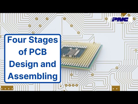 0 Comments 0 Shares 5K Views 0 Reviews
 -
Four Stages of PCB Design and Assembling
#PCBassembly
#PrintedCircuitBoard
#PCBBoard
#PCBAssembly
#smtassembly
#pcbassemblyservices
PCB is a printed circuit board that helps connect different electrical components. The board is a combination of laminated material, and the copper foil laid on a non-conductive substrate.
A PCB is the main part of any electronic device, so it has to be perfect. It should have functional components and microelectronics circuits to perform well. Development of PCB goes through different processes that you should know well. PCB manufacturing has 4 stages, including design, manufacturing, PCB assembly, and PCB testing.
First Stage- Design
PCB design involves different steps, such as schematic design, layout planning, the placement of the components, routing, and manufacturing files.
PCB schematic design: It is a blueprint of PC design that shows all PCB components with symbols. The schematic design is always according to the technical requirements of the user.
Layout planning: After the schematic design, you have to develop the layout of a PCB that includes physical components’ models, the shape of the PCB, and the structure of a PCB.
Placement of components: It involves planning the placement of various components. You decide on the PCB layers according to your requirements. The right placement of the components ensures a flawless board, decreasing the production cost.
First of all, the designer places the fixed components in the layout, including switches and connectors.
Then, the critical components are placed, such as memory chips, microprocessors, as well as power supplies.
Then the supporting components of the PCB are placed, like inductors, capacitors, and resistors.
In the end, the decoupling capacitors and terminating resistors are placed.
Routing: Once the components are placed, you have to connect all components through trace routing. There are four ways to do so, such as manual routing, auto-interactive routing, semi-automatic, and batch-auto routing. You can choose any method according to your Printed Circuit Board and budget.
Design: In this stage, you have to plan for the number of board layers, dimension of the board, and types of components. You can use a special app in this case, such as EDA or electronic design automation. The designer often adopts the SMT instead of a through-hole technology, depending on your requirements.Once the design is over, you can export the design files to CAD or Gerber format.
Preparation of manufacturing files: This is the last stage of design where the designer exports the Gerber files for manufacturing. The manufacturer needs these files to develop a printed circuit board.
Stage 2-Manufacturing of Circuit Board
Once the manufacturer receives all design drawings, he starts making PCB. It involves different stages as described below:
Design Imaging: The manufacturer uses a plotter to convert the PCB design files into filmslike they resemble the photo negatives of the schematic design. The printer uses black and clear inks for inner and outer layers. Copper traces and circuits are shown with black ink, whereas the non-conductive parts are shown with clearink.
Printing of Inner Layers on Copper: It is the initial stage of PCB manufacturing. The engineer uses a substrate material to make a laminated board. Like, epoxy resin or fiberglasses are common in this case. The design of the PCB is printed on the board, and then his pre-bondscopper on a board’s both sides. After that comes the etching of copper, and then the board is protected through a photo-sensitive film.
Ultraviolet Light: the manufacturer then exposes the resist-covered PCB to UV light to strengthen the photo-reactive material. Then the board is cleaned with an alkaline solution to get rid of unnecessary copper particles. The expert checks the board to remove any errors and then goes to the next stage. The main aim of UV blasting is to develop a PCB Board according to the schematic drawing.
Inner layer’s etching: copper’s inner layer needs chemical etching for removal. The process of photoresist prevents the essential copper from etching. The board size determines the amount of the solution and etching time which is less for small boards but more for large boards.
Read more: https://bit.ly/3bUkSaE
Website: https://pnconline.com/
Facebook: https://www.facebook.com/PNCONLINE
Twitter: https://twitter.com/PNCINC
Instagram: https://www.instagram.com/pnc_pcb/
Tumblr: https://www.tumblr.com/blog/view/pncinc
Myspace :https://myspace.com/pncinc2020
Bresdel: https://bresdel.com/pncinc
Pinterest :https://www.pinterest.com.au/rrosh2014/_created/
Call us: (973) 284-1600
Email us: sales@pnconline.com
Location: PNC INC, 115 East Centre St.Nutley, NJ, 07110Four Stages of PCB Design and Assembling #PCBassembly #PrintedCircuitBoard #PCBBoard #PCBAssembly #smtassembly #pcbassemblyservices PCB is a printed circuit board that helps connect different electrical components. The board is a combination of laminated material, and the copper foil laid on a non-conductive substrate. A PCB is the main part of any electronic device, so it has to be perfect. It should have functional components and microelectronics circuits to perform well. Development of PCB goes through different processes that you should know well. PCB manufacturing has 4 stages, including design, manufacturing, PCB assembly, and PCB testing. First Stage- Design PCB design involves different steps, such as schematic design, layout planning, the placement of the components, routing, and manufacturing files. PCB schematic design: It is a blueprint of PC design that shows all PCB components with symbols. The schematic design is always according to the technical requirements of the user. Layout planning: After the schematic design, you have to develop the layout of a PCB that includes physical components’ models, the shape of the PCB, and the structure of a PCB. Placement of components: It involves planning the placement of various components. You decide on the PCB layers according to your requirements. The right placement of the components ensures a flawless board, decreasing the production cost. First of all, the designer places the fixed components in the layout, including switches and connectors. Then, the critical components are placed, such as memory chips, microprocessors, as well as power supplies. Then the supporting components of the PCB are placed, like inductors, capacitors, and resistors. In the end, the decoupling capacitors and terminating resistors are placed. Routing: Once the components are placed, you have to connect all components through trace routing. There are four ways to do so, such as manual routing, auto-interactive routing, semi-automatic, and batch-auto routing. You can choose any method according to your Printed Circuit Board and budget. Design: In this stage, you have to plan for the number of board layers, dimension of the board, and types of components. You can use a special app in this case, such as EDA or electronic design automation. The designer often adopts the SMT instead of a through-hole technology, depending on your requirements.Once the design is over, you can export the design files to CAD or Gerber format. Preparation of manufacturing files: This is the last stage of design where the designer exports the Gerber files for manufacturing. The manufacturer needs these files to develop a printed circuit board. Stage 2-Manufacturing of Circuit Board Once the manufacturer receives all design drawings, he starts making PCB. It involves different stages as described below: Design Imaging: The manufacturer uses a plotter to convert the PCB design files into filmslike they resemble the photo negatives of the schematic design. The printer uses black and clear inks for inner and outer layers. Copper traces and circuits are shown with black ink, whereas the non-conductive parts are shown with clearink. Printing of Inner Layers on Copper: It is the initial stage of PCB manufacturing. The engineer uses a substrate material to make a laminated board. Like, epoxy resin or fiberglasses are common in this case. The design of the PCB is printed on the board, and then his pre-bondscopper on a board’s both sides. After that comes the etching of copper, and then the board is protected through a photo-sensitive film. Ultraviolet Light: the manufacturer then exposes the resist-covered PCB to UV light to strengthen the photo-reactive material. Then the board is cleaned with an alkaline solution to get rid of unnecessary copper particles. The expert checks the board to remove any errors and then goes to the next stage. The main aim of UV blasting is to develop a PCB Board according to the schematic drawing. Inner layer’s etching: copper’s inner layer needs chemical etching for removal. The process of photoresist prevents the essential copper from etching. The board size determines the amount of the solution and etching time which is less for small boards but more for large boards. Read more: https://bit.ly/3bUkSaE Website: https://pnconline.com/ Facebook: https://www.facebook.com/PNCONLINE Twitter: https://twitter.com/PNCINC Instagram: https://www.instagram.com/pnc_pcb/ Tumblr: https://www.tumblr.com/blog/view/pncinc Myspace :https://myspace.com/pncinc2020 Bresdel: https://bresdel.com/pncinc Pinterest :https://www.pinterest.com.au/rrosh2014/_created/ Call us: (973) 284-1600 Email us: sales@pnconline.com Location: PNC INC, 115 East Centre St.Nutley, NJ, 071100 Comments 0 Shares 5K Views 0 Reviews


More Stories