

Semiconductor Inspection Microscope: Precision in Microchip Quality Assurance
The semiconductor inspection microscope is an essential tool in the semiconductor industry, enabling precise examination and quality control of microchips and other semiconductor devices. These microscopes are designed to detect defects, irregularities, and contaminants at microscopic levels, ensuring that only flawless components proceed to the next stage of production. As the semiconductor industry continues to advance, the need for high-resolution, accurate, and reliable inspection tools like these microscopes is more critical than ever.
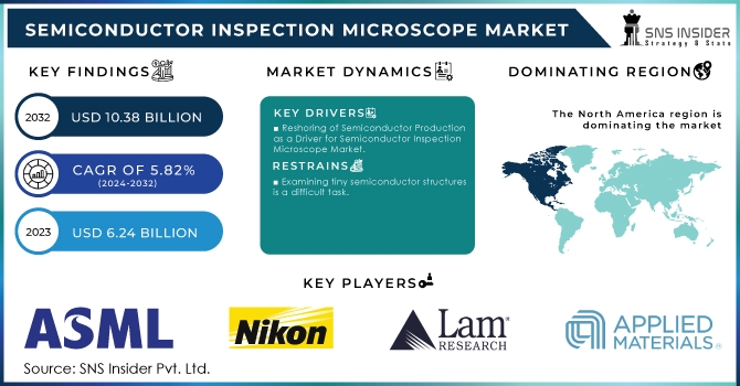
The Semiconductor Inspection Microscope Market was valued at USD 6.24 billion in 2023 and is projected to reach USD 10.38 billion by 2032, growing at a CAGR of 5.82% during the forecast period from 2024 to 2032.
Future Scope:
The future of semiconductor inspection microscopes lies in increasing resolution and automation. As microchips continue to shrink in size and increase in complexity, inspection microscopes will need to offer even greater magnification and precision. Additionally, the integration of artificial intelligence (AI) and machine learning (ML) algorithms into these systems will allow for faster, more accurate defect detection and classification. This automation will not only improve inspection efficiency but also reduce the likelihood of human error, further enhancing the quality and reliability of semiconductor devices.
Trends:
Several trends are shaping the semiconductor inspection microscope market. The push for higher resolution and faster inspection times is driving the development of new imaging technologies, such as multi-beam electron microscopy and advanced optical systems. The growing complexity of semiconductor devices, including 3D ICs and advanced packaging techniques, is also creating demand for inspection microscopes capable of analyzing multi-layered structures. Moreover, the increasing adoption of automation and AI in semiconductor manufacturing is leading to more sophisticated inspection systems that can autonomously identify and categorize defects with minimal human intervention.
Applications:
Semiconductor inspection microscopes are used throughout the semiconductor manufacturing process, from wafer fabrication to final assembly. They are essential for detecting defects in photomasks, wafers, and finished microchips, ensuring that only components meeting the highest quality standards are delivered to customers. These microscopes are also used in research and development (R&D) settings to study the effects of new materials and processes on semiconductor performance. Additionally, semiconductor inspection microscopes play a crucial role in failure analysis, helping engineers understand the root causes of defects and improve manufacturing processes.
Solutions and Services:
Manufacturers of semiconductor inspection microscopes offer a range of products designed to meet the specific needs of different stages of semiconductor production. These include high-resolution optical microscopes, electron microscopes, and specialized inspection systems for photomasks and wafers. In addition to the microscopes themselves, many providers offer integrated software solutions for defect detection, classification, and data analysis. Comprehensive support services, including training, calibration, and maintenance, ensure that inspection systems continue to deliver accurate and reliable results throughout their operational life.
Key Points:
· Semiconductor inspection microscopes are critical tools for ensuring the quality and reliability of microchips and semiconductor devices.
· Future advancements will focus on higher resolution, automation, and the integration of AI and ML for faster and more accurate inspections.
· Key applications include wafer fabrication, photomask inspection, R&D, and failure analysis.
· Market trends include the development of new imaging technologies, multi-layered structure analysis, and increased automation.
· Solutions and services include high-resolution optical and electron microscopes, defect detection software, and comprehensive support.
Read More Details: https://www.snsinsider.com/reports/semiconductor-inspection-microscope-market-4234
Contact Us:
Akash Anand — Head of Business Development & Strategy
Email: info@snsinsider.com
Phone: +1–415–230–0044 (US) | +91–7798602273 (IND)