

The manufacturing process of silicon wafers involves a series of steps. These processes are used to make the components needed for semiconductor devices. The first step of silicon wafer manufacturing is a fabrication. This step involves cutting and polishing the wafers. The cutting and polishing process creates a sharp edge that is needed to ensure high-quality device performance.
The second step is the double side grinding, which is performed to remove saw marks, improve TTV, and flatness. This step is followed by the chemical etching process. This process uses acid or basic solutions to remove the layer that was created by the previous slicing.
The next step in silicon wafer manufacturing is to introduce the dopants into the wafer. These substances are elements from Groups 3 and 4, and they control the properties of the silicon wafer.
These dopants can be Boron, Phosphorus, Arsenic, Antimony, and Phosphorous. In some cases, the dopants are N or P-type. The process is repeated until the silicon wafer is complete.
The third step in silicon wafer manufacturing involves adding the dopants, which are chemical compounds from Groups 3 and 4 of the periodic table. These chemicals determine the electrical and magnetic properties of the silicon wafer material.
Dopants are available as N or P-type, so if you use one, it will depend on the composition of the material. Dopants can be used to make a semiconductor wafer with a certain property.
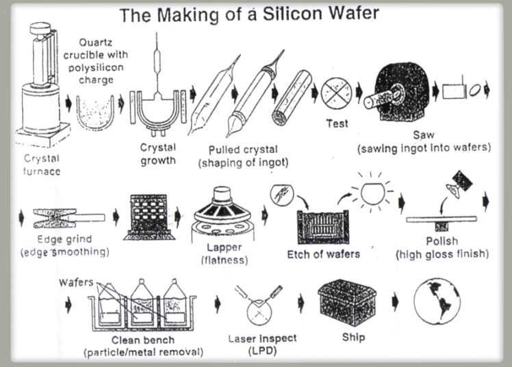
The Czochralski method is the simplest and most basic way to make silicon wafers. In this method, a solid piece of silicon is placed in a bath of polycrystalline silicon and molten.
As the liquid grows, it slowly pulls the solid inward, creating a cylindrical ingot. Afterward, the finished wafer will be a round disc. So, it is not uncommon for the silicon wafer manufacturing process to last for decades.
The third step of silicon wafer manufacturing involves the polishing process. In this step, the ingot is fully grown and ground to a rough diameter. A notch is used to mark its orientation.
The silicon ingot is then cut using a diamond edge saw. The diamond edge saw prevents the silicon wafer from bowing or warping during the process. Once the polishing is completed, the silicon ingot is ready to be soldered.
The fourth step involves the polishing of the silicon wafers. After the silicon wafer is sliced, it needs to have a mirror-like surface. To accomplish this, the silicon wafer is held in a vacuum carrier and is rotated using a rotating polishing pad.
After the polishing, the wafer is packaged under a vacuum. These processes are done by the process of slicing a silicon wafer.
The fourth step involves the polishing of the silicon wafers. The silicon ingot is fully grown. Once the ingot is shaped, it is sliced to a rough size diameter. The diamond edge saw is used to avoid damage to the silicon.
It is important to ensure that the surface of the silicon is wettable after the polishing process. If a wafer is not wettable, it will break down during the manufacturing process.
The fourth step is nitriding. Nitridation is a chemical process that involves the formation of silicon layers. The process is known as "nitriding" because the silicon is coated with a thin film of nitriding agents.
During this step, the nitridation of the silicon layer is complete. This chemical process is the final step in the manufacturing of semiconductor wafer. This phase has many steps and requires a very high temperature.
The process involves a series of processes. The first step is to separate the crystals. The second step is to separate them into wafers. These steps are called photolithography.
They use light to transfer patterns to a silicon wafer. Once the crystals have been separated, they are polished to an atomic level. The third step is the etching of the silicon wafers. This process is called sintering.